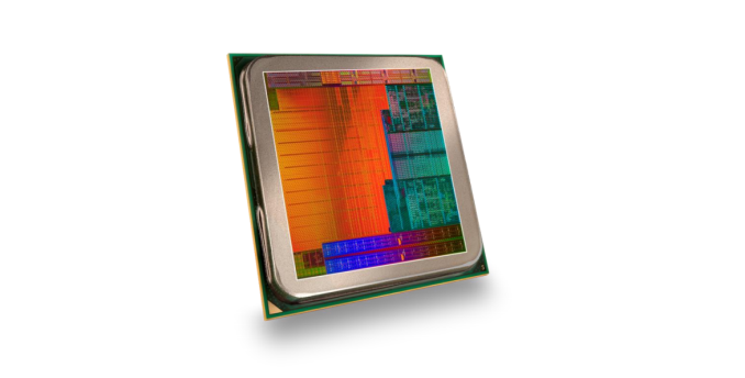
The first major component launch of 2014 falls at the feet of AMD and the next iteration of its APU platform, Kaveri. Kaveri has been the aim for AMD for several years, it's actually the whole reason the company bought ATI back in 2006. As a result many different prongs of AMD’s platform come together: HSA, hUMA, offloading compute, unifying GPU architectures, developing a software ecosystem around HSA and a scalable architecture. This is, on paper at least, a strong indicator of where the PC processor market is heading in the mainstream segment. For our Kaveri review today we were sampled the 45/65W (cTDP) A8-7600 and 95W A10-7850K Kaveri models. The A10-7850K is available today while the A8 part will be available later in Q1.
The Kaveri Overview
To almost all users, including myself up until a few days ago, Kaveri is just another iteration of AMD’s APU line up that focuses purely on the integrated graphics side of things, while slowly improving the CPU side back to Thuban levels of performance. Up until a few days ago I thought this too, but Kaveri is aiming much higher than this.
Due to the way AMD updates its CPU line, using the ‘tick-tock’ analogy might not be appropriate. Kaveri is AMD’s 3rd generation Bulldozer architecture on a half-node process shrink. Kaveri moves from Global Foundries' 32nm High-K Metal Gate SOI process to its bulk 28nm SHP (Super High Performance) process. The process node shift actually explains a lot about Kaveri's targeting. While the 32nm SOI process was optimized for CPU designs at high frequency, GF's bulk 28nm SHP process is more optimized for density with a frequency tradeoff. AMD refers to this as an "APU optimized" process, somewhere in between what a CPU and what a GPU needs. The result is Kaveri is really built to run at lower frequencies than Trinity/Richland, but is far more dense.
Kaveri is the launch vehicle for AMD's Steamroller CPU architecture, the 3rd iteration of the Bulldozer family (and second to last before moving away from the architectural detour). While Piledriver (Trinity/Richland) brought Bulldozer's power consumption down to more rational levels, Steamroller increases IPC. AMD uses Steamroller's IPC increase to offset the frequency penalty of moving to 28nm SHP. AMD then uses the density advantage to outfit the design with a substantially more complex GPU. In many senses, Kaveri is the embodiment of what AMD has been preaching all along: bringing balance to the CPU/GPU split inside mainstream PCs. The strategy makes a lot of sense if you care about significant generational performance scaling, it's just unfortunate that AMD has to do it with a CPU architecture that puts it at a competitive deficit.
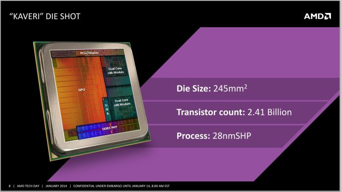
The die of Kaveri is of similar size to Richland (245mm2 vs 236mm2) but has 85% more transistors (2.41B vs. 1.3B). Unfortunately AMD hasn't confirmed whether we are talking about layout or schematic transistors here, or even if both figures are counted the same way, but there's clearly some increase in density. Typically a move from 32nm to 28nm should give a 26% boost for the same area, not an 85% boost.
The GPU side of the equation is moving from a Cayman derived GPU in Richland to a Hawaii / GCN based one in Kaveri with the addition of HSA support. This vertically integrates the GPU stack to GCN, allowing any improvements in software tool production to affect both.
For the first time since AMD went on its march down APU lane, the go-to-market messaging with Kaveri is heavily weighted towards gaming. With Llano and Trinity AMD would try to mask CPU performance difficiencies by blaming benchmarks or claiming that heterogeneous computing was just around the corner. While it still believes in the latter, AMD's Kaveri presentations didn't attempt to force the issue and instead focused heavily on gaming as the killer app for its latest APU. HSA and heterogeneous computing are still important, but today AMD hopes to sell Kaveri largely based on its ability to deliver 1080p gaming in modern titles at 30 fps. Our testing looks favourably on this claim with some titles getting big boosts over similar powered Richland counterparts, although the devil is in the details.
The feature set from Richland to Kaveri gets an update all around as well, with a fixed function TrueAudio DSP on the processor to offload complex audio tasks – AMD claims that reverb added to one audio sample for 3+ seconds can take >10% of one CPU core, so using the TrueAudio system allows game developers to enhance a full surround audio with effects, causing more accurate spatialization when upscaling to 7.1 or downscaling to stereo from 5.1. TrueAudio support unfortunately remains unused at launch, but Kaveri owners will be able to leverage the technology whenever games launch with it. Alongside TrueAudio, both the Unified Video Decoder (UVD) and the Video Coding Engine (VCE) are upgraded.
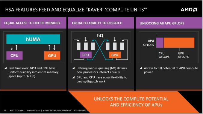
One of the prominent features of Kaveri we will be looking into is its HSA (Heterogenous System Architecture) – the tight coupling of CPU and GPU, extending all the way down to the programming model. Gone are the days when CPU and GPU cores have to be treated like independent inequals, with tons of data copies back and forth for both types of cores to cooperate on the same problem. With Kaveri, both CPU and GPU are treated as equal class citizens, capable of working on the same data in the same place in memory. It'll be a while before we see software take advantage of Kaveri's architecture, and it's frustrating that the first HSA APU couldn't have come with a different CPU, but make no mistake: this is a very big deal.The big push on AMD’s side is the development of tools for the major languages (OpenCL, Java, C++ and others) as well as libraries for APIs to do this automatically and with fewer lines of code.
Kaveri will support OpenCL 2.0, which should make it the first CPU/APU/SoC to carry that certification.
The Kaveri Lineup: Desktop Sweet Spot at 45W
For years now Intel has been targeting mobile first with its CPU architectures. More recently NVIDIA started doing the same with its GPUs (well, ultra-mobile first). With Haswell, Intel's architecture target shifted from 35 - 45W down to 10 - 20W, effectively making Ultrabook form factors the target for its CPU designs. Intel would then use voltage scaling to move the architecture up/down the stack, with Atom and Quark being used to go down to really low TDPs.
For AMD, Kaveri truly embraces the mobile first approach to design with a platform target of 35W. AMD is aiming higher up the stack than Intel did with Haswell, but it also has a lower end CPU architecture (Jaguar) that shoots a bit above Atom. I suspect eventually AMD will set its big architecture sights below 35W, but for now AMD plays the hand it was dealt. The Kaveri project was started 4 years ago and the Haswell platform retargeting was a mid-design shift (largely encouraged by Apple as far as I can tell), so it's not surprising to see Kaveri end up where it does. It's also worth pointing out that the notebook designs AMD primarily competes in are larger 35W machines anyways.
AMD's mobile roadmap states that we'll see Kaveri go all the way down to 15W (presumably in a 2-core/1-module configuration):
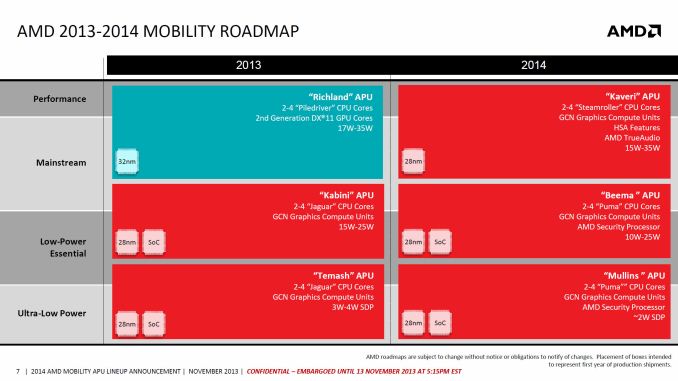
Kaveri mobile however appears to be a mid 2014 affair; what launches today are exclusively desktop parts. With an aggressive focus on power consumption, AMD's messaging around Kaveri is simply more performance at the same power.
Here are the Bulldozer based processors for each of AMD’s main desktop target segments: 45W, 65W and 95-100W:

Actually, the 45W segment is almost a cop out here. AMD never released a 45W desktop edition of Trinity, and while it formally released a couple of 45W Richland APUs back in August, I literally have not seen them for sale in the regular markets (US, UK) that I check. After my initial Kaveri pre-launch information article, one reader got in touch and confirmed that a mid-sized Italian etailer was selling them and had some in stock, but the majority of the world can't seem to get a hold of them. For the purpose of this review, AMD was kind enough to source retail versions of both the A8-6500T and A8-6700T for comparison points to show how much the system has improved at that power bracket.

By comparison, AMD has a history of making 65W CPUs. You may notice that the Kaveri model listed is the same model listed in the 45W table. This is one of the features of AMD’s new lineup – various models will have a configurable TDP range, and the A8-7600 will be one of them. By reducing the power by about a third, the user sacrifices a margin of CPU base speed and turbo speed, but no reduction in processor graphics speeds. At this point in time, the A8-7600 (45W/65W) is set for a Q1 release rather than a launch day release, and we have not received details of any further configurable TDP processors.

Here we see the 32nm SOI to bulk 28nm SHP shift manifesting itself in terms of max attainable frequency. Whereas the A10-6800K ran at 4.1/4.4GHz, the A10-7850K drops down to 3.7/4.0GHz (base/max turbo). TDP falls a bit as well, but it's very clear that anyone looking for the high end of AMD's CPU offerings to increase in performance won't find it with Kaveri. I suspect we'll eventually see an AMD return to the high-end, but that'll come once we're done with the Bulldozer family. For now, AMD has its sights set on the bulk of the mainstream market - and that's definitely not at 95/100W.
Kaveri Motherboard/Socket Compatibility
AMD’s socket and chipset situation with Kaveri also adjusts slightly, maintaining a small difference to Richland. The new APUs will only fit into an FM2+ socket motherboard, which differs from FM2 by two pins, and Richland/Trinity APUs will also fit into FM2+. However, Kaveri APUs will not fit into any older FM2 motherboards. On the chipset side, AMD is adding the A88X chipset to the Bulldozer chipset family, complementing A55, A75 and A85X. Similar to Trinity and Richland, the chipset is not a definitive indicator of the socket of the motherboard, except for A88X: A88X will only appear on FM2+ motherboards.
AMD has the workings of a potential platform changer, and certainly the programming paradigm change from ‘normal’ to HSA is one that is going to be at the forefront of AMD’s APU production for the foreseeable future.
Thank's To : www.anandtech.com & www.youtube.com
No comments:
Post a Comment